
Product Code :Product Name :Stock : |
11107Fully Controlled Rectifier Available
|

|
Option-1 : Buy this Product as it is
Option-2 : Buy this Product With Your Identity / Name / Brand
Option-3 : Customize the features of this Product as per your Need
Make Changes in the board, add or remove the features that you want. Customize this board as per your need and send us the specifications so that we can process the board and deliver them exactly as per your requirement.
Boards Will be designed with your brand name. No Manufacturer Identity. Minimum Order Quantity = 10 |
|
Product Information

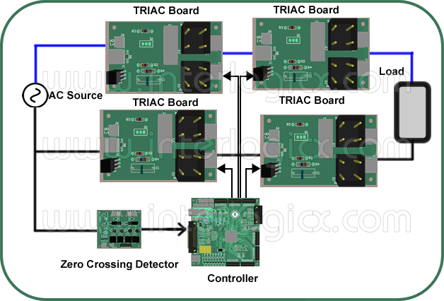
Hardware Requirements:
The following hardware’s are required to realize a fully controlled rectifier.
1. Stable AC source,
2. Four switch TRIAC switch boards.
3. Controller Section (uC or FPGA),
4. Zero Crossing Detector,
5. Isolated TRIAC gate driver,
6. Load.
Working Principle:
The ZCD circuitry is designed to identify the exact zero crossing point of an input ac signal (say 50Hz). Using the reference signal from the ZCD circuitry the corresponding TRIAC switches should be triggered to pass on the corresponding AC wave to the load directly.
Isolated TRIAC gate driver is used to provide isolation between the controller section and the TRIAC high power circuitry. Isolated TRIAC gate driver IC in itself contains a miniature TRIAC inside of it. TRIAC cannot be turned on by applying DC voltage at its gate terminal; hence the input ac voltage itself is used to turn on the TRIAC by applying the ac voltage to its gate terminal. After the zero cross the pulse applied from the controller triggers the internal isolated TRIAC to pass the AC voltage in to the main TRIAC switch’s gate terminal. Once the ac voltage is applied to the TRIACs gate terminal it starts conducting until the AC voltage across the terminal MT1 and MT2 is zero. Once the TRIAC switch starts conducting, TRIAC switch cannot be turned off by turning off the trigger pulse from the controller. TRIAC switch will only stop conducting when the ac signal across the terminal MT1 and MT2 crosses zero.
In a fully controlled rectifier we are replicating the characteristics of a full bridge diode rectifier but with the ability to control the output. So in a full bridge diode rectifier during positive half cycle of the input ac, diagonally opposite diodes D1 & D4 conduct and during the negative half cycle diodes D2 & D3 conduct to produce a full wave DC at the output.
Likewise during the positive voltage level (or rising edge) of the ZCD, TRIAC switches T1 & T4 should be turned ON to make available the input voltage at the output, during the negative voltage level (or falling edge) switches T2&T3 should be turned to produce a full wave DC at the output load.
For controlled rectifier operation, say for 10% voltage reduction at the output. TRIAC switches must be turned ON after a delay of 10% from the time of ZCD cross over pulses for both positive and negative half cycles of the input AC voltage.
