
Product Code :Product Name :Stock : |
11106Buck Boost Converter Available
|

|
Option-1 : Buy this Product as it is
Option-2 : Buy this Product With Your Identity / Name / Brand
Option-3 : Customize the features of this Product as per your Need
Make Changes in the board, add or remove the features that you want. Customize this board as per your need and send us the specifications so that we can process the board and deliver them exactly as per your requirement.
Boards Will be designed with your brand name. No Manufacturer Identity. Minimum Order Quantity = 10 |
|
Product Information

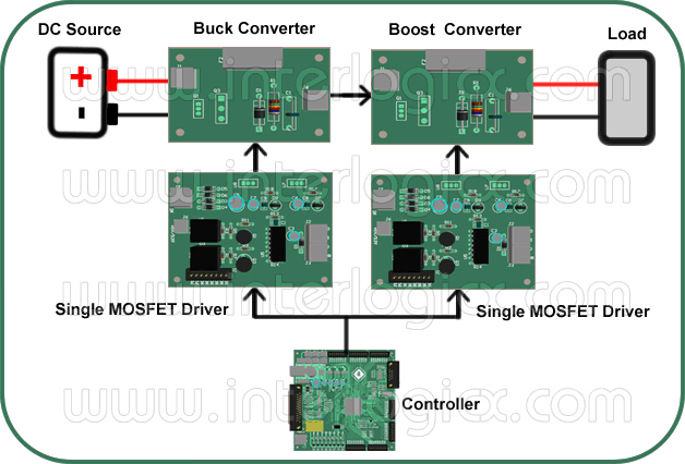
Hardware Requirements:
The following hardware’s are required to realize a dc to dc buck converter.
1. Constant DC source,
2. Single switch MOSFET board – Two numbers one acts as buck switch and the other as boost switch.
3. Inductor,
4. Controller Section (uC or FPGA),
5. Isolated MOSFET Gate Driver – Two Numbers for buck and boost switches,
6. Load.
Working Principle:
A typical dc to dc buck boost converter has two separate switches for buck and boost operations.
For voltage buck operations, the buck switch is connected in series between the voltage source and the load via an inductor. A freewheeling diode is connected in between the buck switch and the inductor for the purpose of providing a closed circuit path when the buck switch is turned off. The boost switch must be turned off for continuous buck operation.
For voltage boost operations, MOSFET switch should be connected after the inductor. A high voltage diode should be connected in forward bias between the filter cap + load and the MOSFET switch. A diode is placed in order to prevent the filter cap from consuming the power during the MOSFET ON period. Hence achieving voltage boost at the output. During boost operation the buck switch should be fully turned ON.
