
Product Code :Product Name :Stock : |
11105Boost Converter Available
|

|
Option-1 : Buy this Product as it is
Option-2 : Buy this Product With Your Identity / Name / Brand
Option-3 : Customize the features of this Product as per your Need
Make Changes in the board, add or remove the features that you want. Customize this board as per your need and send us the specifications so that we can process the board and deliver them exactly as per your requirement.
Boards Will be designed with your brand name. No Manufacturer Identity. Minimum Order Quantity = 10 |
|
Product Information

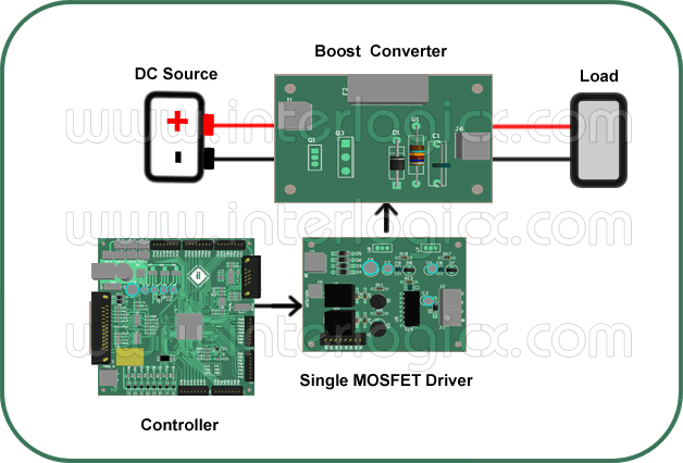
Hardware Requirements:
The following hardware’s are required to realize a dc to dc boost converter.
1. Constant DC source,
2. Single switch MOSFET board.
3. Boost Inductor,
4. Controller Section (uC or FPGA),
5. Isolated MOSFET Gate Driver,
6. Load.
Working Principle:
A MOSFET based DC to DC boost converter has an inductor, which acts as the energy storage element in the boost circuit. Capacitor discharge blocking diode should be connected properly in series with inductor and load. Without the blocking diode our boost converter circuit will not achieve voltage boosting.
Duty-cycle or On-time of the MOSFET switch determines the increase in voltage at the output. MOSFET should never be turned fully on or fully off. 100% duty cycle on the MOSFET would result in a blown out circuit, 0% duty cycle on the MOSFET does not give any voltage at the output.
Depending on the duty cycle of the pulse width given to the gate terminal of the MOSFET switch, the boosted voltage at the output varies. Inductor value should be chosen carefully based upon voltage level desired at the output.
